4 nm

Samsung Elect
2026-09-22 06:50:51

Samsung weighs 4 nm foundry expansion as HBM4 base chip demand rises

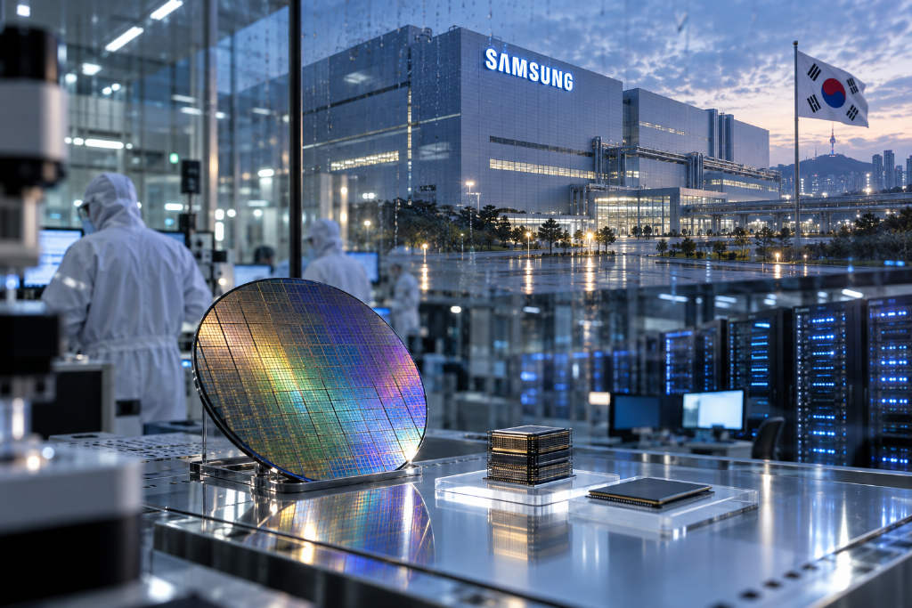
Samsung Electronics is reviewing an expansion of its 4 nm foundry capacity as demand for HBM4 base chips increases, according to a Sept. 21 report by Money Today cited by ChainCatcher. The company is pushing ahead with advanced-process capacity growth as the HBM market expands. Samsung’s HBM4 combines a 10 nm-class sixth-generation (1c) DRAM core die with a 4 nm logic base die that handles high-speed data exchange with GPUs and other AI accelerators. Unlike SK hynix, which uses TSMC’s 12 nm process for its HBM4 base chip, Samsung is using its own 4 nm node. The report said Samsung’s relevant production line is already running at full capacity and has taken orders tied to Nvidia Groq 3 LPUs. Samsung has also recently raised prices for new 4 nm orders and HBM4 base chips. The company expects third-quarter HBM4 revenue to rise by more than three times from the previous quarter, with HBM4 accounting for well above 60% of HBM revenue in the second half. It is also evaluating a new 2 nm line for HBM5.
70
Samsung weighs 4 nm foundry expansion as HBM4 base chip demand rises
TSMC
2026-09-21 00:22:34

TSMC speeds up Central Taiwan fab buildout for A14 process, report says

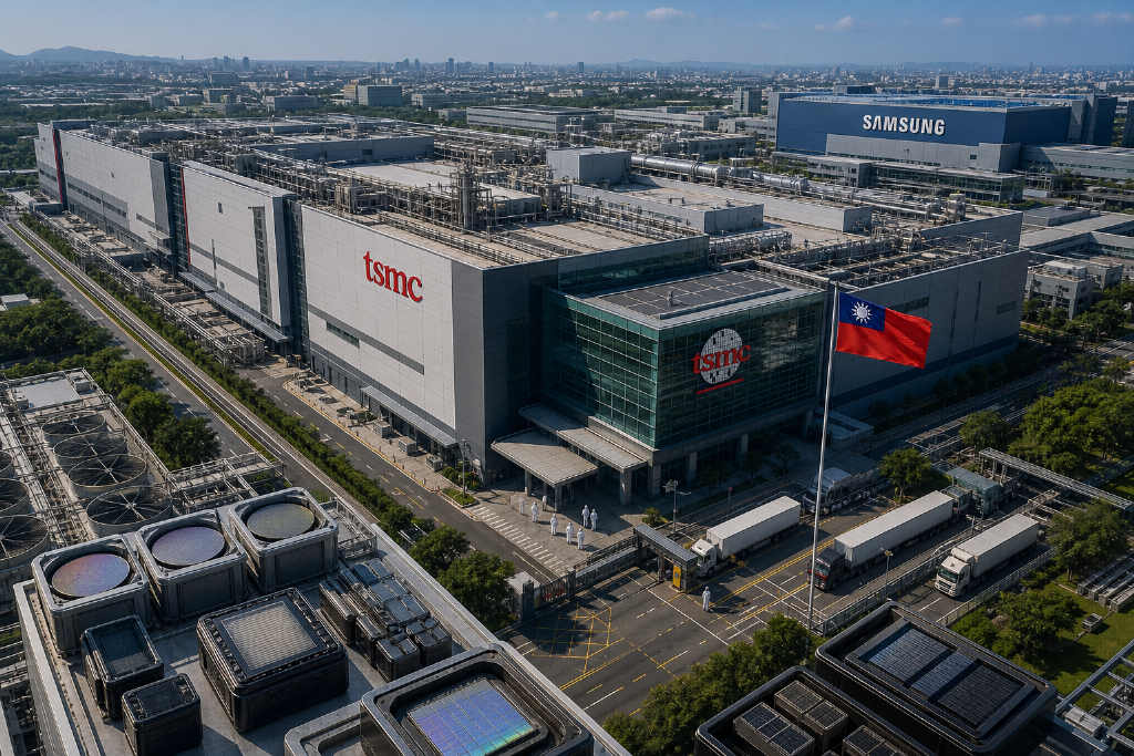
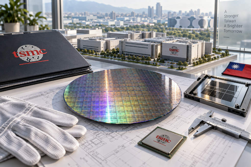
Taiwan Semiconductor Manufacturing Co. is accelerating construction of four fabs in Central Taiwan Science Park to support its 1.4-nanometer A14 process, according to a report cited by ChainCatcher from Commercial Times. As of early September 2026, work on the Phase 2 P1 plant was progressing smoothly, with completion expected in April 2027, followed by equipment move-in and trial production. The P2 plant is moving ahead in parallel and is expected to complete equipment tuning with P1 and reach readiness for mass production before the end of 2027. The report said all four 1.4 nm wafer fabs at the site are expected to be completed in the second quarter of 2028 and enter large-scale mass production. Major customers said to have reserved A14 capacity include Apple, NVIDIA, AMD, Qualcomm, MediaTek, Broadcom and cloud service providers. Monthly capacity is estimated at 120,000 to 160,000 12-inch wafers, with projected annual revenue contribution to TSMC of $45 billion to $52 billion.

170
TSMC speeds up Central Taiwan fab buildout for A14 process, report says
Fujitsu
2026-09-15 03:51:35

Fujitsu starts sales of MONAKA AI CPU and unveils Japan-made server line

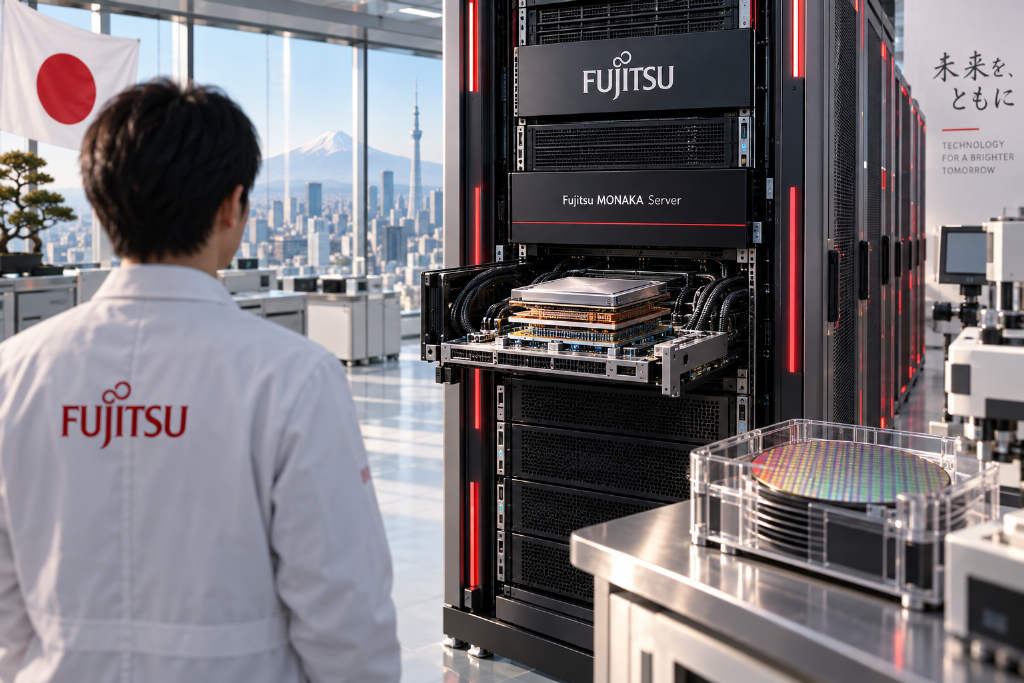
Fujitsu said on Sept. 14 that it will begin selling its in-house next-generation CPU, FUJITSU-MONAKA, and introduced the Fujitsu MONAKA Server built around the chip. The company said the processor is being mass-produced on TSMC’s 2 nm process and draws on technology developed through Fugaku, the supercomputer jointly built by Fujitsu and Japan’s RIKEN. Fujitsu described MONAKA as the first CPU to combine a 2 nm process with a 3D stacked design, using 2 nm for compute cores and 5 nm for cache and I/O under a heterogeneous integration approach. The Arm-based chip supports SVE2, runs at up to 3.8 GHz, and offers a memory transfer rate of 8800 MT/s. In AI inference workloads, Fujitsu said dedicated matrix instructions allow MONAKA to deliver twice the inference throughput of competing CPUs in the same category. The company also highlighted Arm CCA confidential computing support for protecting data and applications in memory across cloud and multi-tenant environments. Fujitsu plans to ship the CPU globally from November to cloud providers, data center operators and server makers. It said 24 Japanese financial and telecom companies have already deployed test units, while more than 40 companies are in talks. Fujitsu also said it has signed a supply agreement with SuperMicro and plans to enter the U.S. and Asian markets in 2027.

610
Fujitsu starts sales of MONAKA AI CPU and unveils Japan-made server line
Samsung Elect
2026-09-11 05:26:42

Samsung’s 2 nm yield climbs past 70%, but Qualcomm foundry order remains stalled over pricing

Samsung Electronics has improved the yield of its 2 nm gate-all-around process to above 70%, up from below 50% at the start of the year, according to a Sept. 11 report cited by South Korean media. Its 4 nm yield was reported at above 80%. Even so, a potential foundry deal with Qualcomm for a 2 nm application processor has been delayed because the two sides have not agreed on pricing, with local outlet The Bell saying mass production within this year is now difficult. KB Securities said the stabilization of advanced-node yields could help Samsung’s foundry business return to profit from the third quarter of 2026. The report also linked the 2 nm improvement to Samsung’s competitiveness in HBM base dies. Separately, KB Securities projected Samsung’s HBM market share to rise from 33% in the second quarter to around 40% in the fourth quarter, with third-quarter HBM4 revenue expected to grow by more than three times quarter over quarter. Samsung is already mass-producing HBM4, offering seventh-generation HBM4E samples, and extending its roadmap to HBM5 and zHBM.

1120
Samsung’s 2 nm yield climbs past 70%, but Qualcomm foundry order remains stalled over pricing
Donald Trump
2026-09-09 01:14:40

Crypto roundup: Trump defends his stock trading, YZi Labs ranks No. 2 among active family offices in August

A wide set of crypto, regulatory and corporate developments landed over the past 24 hours, led by a new post from U.S. President Donald Trump, fresh family-office investment data, enforcement action in Australia, and a string of market and infrastructure updates across Bitcoin, DeFi and payments. Trump said on Truth Social that he had made "hundreds of billions of dollars" for the United States through stocks and other assets and added that he was doing it "for our country, not for myself." Reuters had previously reported that ethics filings showed Trump disclosed at least $220 million and as much as roughly $750 million in personal securities trades in the first three months of 2026. On the investment side, FINTRX data cited by Jiaoban Xinzhi Dian showed that Binance founder Changpeng Zhao’s YZi Labs ranked as the world’s second-most active family office in August, taking part in 10 funding rounds with a combined disclosed round size of $42.1 million. The same dataset showed family offices participated in 109 deals during the month, with disclosed financing totaling $16.9 billion. Elsewhere, Australia’s AUSTRAC said it had canceled, suspended or refused to renew registrations for 45 crypto and remittance businesses over the past year. Market commentary from Two Prime and Wintermute focused on Bitcoin’s rebound, ETF inflows and key price levels, while other developments included Liquid Network fund returns, Cronos’ rollback after the Tectonic exploit, Circle’s deal for Tazapay, and broader stablecoin and banking moves in Brazil, Switzerland and South Korea.

410
Crypto roundup: Trump defends his stock trading, YZi Labs ranks No. 2 among active family offices in August
Samsung
2026-09-09 12:35:13

Samsung’s Taylor fab books out 2 nm capacity before startup, with Tesla, Broadcom and Arm named as customers

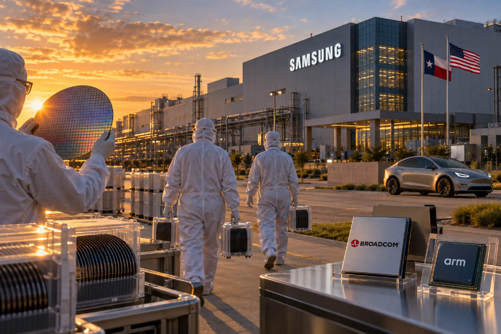
Samsung’s wafer fab in Taylor, Texas has already allocated its baseline 2 nanometer capacity before operations begin, according to a Sept. 8 report by BusinessKorea. The report said the site’s monthly capacity of 50,000 wafers has been fully booked by customers, with pilot production possibly starting as early as the end of September. Among the customers identified in the report are Tesla, Broadcom and Arm. The reported orders cover several product categories: Tesla’s next-generation AI chip AI5, Broadcom’s next-generation communications semiconductor, and Arm’s AI chip for smart devices. Samsung has invested about $37 billion in the Taylor facility since construction began in 2022. Mass production is scheduled for 2027. BusinessKorea also said Samsung’s 2 nm yield improved from about 60% at the beginning of this year to the 80% range, a level described as suitable for mass production. The report linked that improvement to stabilized yields in advanced processes including 4 nm and 5 nm. A second Taylor plant is expected to break ground by the end of this year, with mass production targeted for 2030.

190
Samsung’s Taylor fab books out 2 nm capacity before startup, with Tesla, Broadcom and Arm named as customers
semiconductor
2026-09-02 12:13:13

China’s chip equipment push moves into tougher territory as metrology advances and bottlenecks persist

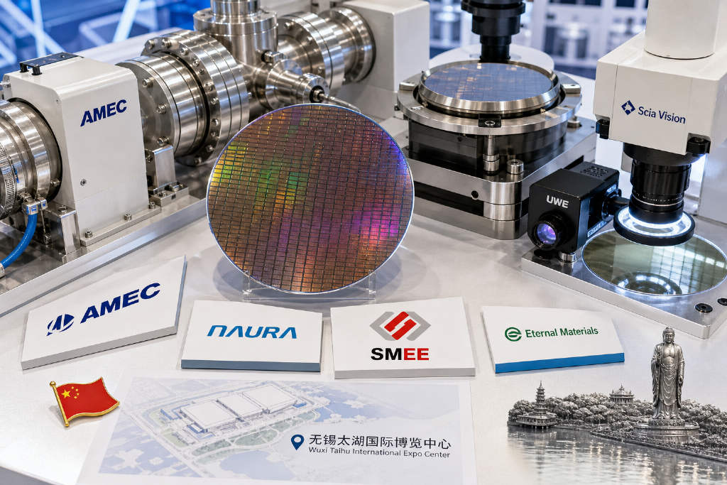
China’s semiconductor equipment industry is entering a more demanding phase, with the easiest import-substitution wins largely behind it and harder categories now drawing the most attention. At CSEAC 2026 in Wuxi, equipment makers and component suppliers used the show to present where domestic progress stands across process tools, metrology and inspection systems, advanced packaging, and core parts. In process equipment, companies such as Advanced Micro-Fabrication Equipment Inc. China (AMEC), NAURA, and Shanghai Micro Electronics Equipment showed continued expansion across etch, deposition, and lithography-related systems. But ion implanters remain a major weak spot. According to data cited by Aion Semiconductor, overall localization in ion implantation is still below 15%, with high-current tools below 10% and high-energy tools largely blank. Metrology and inspection appear to be moving faster. eGenerate, Yuwei Semiconductor, and SDRA were among the companies highlighted for equipment already in volume delivery or advanced validation. In advanced packaging, wafer-to-wafer bonding is more mature, while die-to-wafer bonding is still largely in validation. The report also points to continued progress in domestic core components, arguing that the sector is shifting from isolated breakthroughs toward broader ecosystem building, even as trust barriers, validation constraints, and long R&D cycles remain in place.

960
China’s chip equipment push moves into tougher territory as metrology advances and bottlenecks persist
TSMC
2026-09-01 00:24:45

TSMC seen raising process prices after Samsung moves first on foundry quotes

Samsung Electronics has raised prices for some advanced and mature process nodes, and the market now expects Taiwan Semiconductor Manufacturing Co. (TSMC) to follow with broader increases. According to a report cited by ChainCatcher from Anue, TSMC’s process pricing could rise by 10% to 15% across multiple nodes. TrendForce and Nomura reports said TSMC had already completed a new round of pricing talks with customers in the middle of this year, with some supply-constrained 3 nm N3 process capacity for the second half seeing increases of as much as 15%. Market expectations extend beyond that. By early 2027 at the latest, prices for advanced nodes including N2, N3 and N5 could climb another 5% to 10%. Mature nodes such as N12, N16 and N28, which have not seen price increases for three straight years, may also move higher by as much as 10%. The report also said nearly all N2 and N3 capacity has been booked by Apple and NVIDIA. Separately, CLSA estimates TSMC’s capital expenditure will reach $80 billion in 2027 and $90 billion in 2028, after this year’s capex was raised to $52 billion to $56 billion. TSMC also announced in July that it would expand its U.S. investment to $265 billion.

750
TSMC seen raising process prices after Samsung moves first on foundry quotes